Semiconductor Lithography Systems
- Overview
Products such as smartphones and appliances are becoming smaller and more versatile, and are now part of everyday life. Semiconductor lithography technology is making a significant contribution to the development of semiconductors (semiconductor integrated circuits), which are an integral component of these products.
A semiconductor lithography system is a projection system that transfers a pattern from a photomask to a silicon substrate, also known as a wafer. The process involves:
- Drawing complex circuit patterns on a large glass plate
- Reducing the patterns using ultra-high-performance lenses
- Exposing the patterns onto the wafer
Lithography is used in semiconductor manufacturing to project a pattern onto a material as an outline for the next manufacturing step. For semiconductor chips, a huge drawing of a single chip at its various stages is reduced in size to fractions of an inch, and repeated over the size of the chip wafer.
The most common lithography methods are: Optical lithograph, E-beam lithography.
- Semiconductor Lithography Systems
Semiconductor lithography systems use a process that uses ultra-high-performance lenses to shrink highly complex circuit patterns drawn on photomasks made of large plates of glass and expose them onto silicon substrates called wafers.
Semiconductor lithography systems require three key technologies that determine their performance.
- The first technology is "the resolution capability of the projection lens". The better the resolution of the lens, the more complex the circuit pattern will be when optically transferring it.
- The second technology is "alignment accuracy". To produce a single semiconductor, the photomask must be replaced dozens of times, and the circuit pattern must be etched repeatedly during the exposure process. Therefore, it is critical that the silicon wafer and photomask are perfectly aligned every time.
- The third important component is "throughput". This technology is very important when semiconductors are mass-produced. Throughput is a measure of productivity, expressed as the number of wafers that can be exposed in an hour.
- Optical Lithography
Photolithography, also called optical lithography or UV lithography, is a process used in microfabrication to pattern parts on a thin film or the bulk of a substrate (also called a wafer).
It uses light to transfer a geometric pattern from a photomask (also called an optical mask) to a photosensitive (that is, light-sensitive) chemical photoresist on the substrate. A series of chemical treatments then either etches the exposure pattern into the material or enables deposition of a new material in the desired pattern upon the material underneath the photoresist. In complex integrated circuits, a CMOS wafer may go through the photolithographic cycle as many as 50 times.
Photolithography shares some fundamental principles with photography in that the pattern in the photoresist etching is created by exposing it to light, either directly (without using a mask) or with a projected image using a photomask.
This procedure is comparable to a high precision version of the method used to make printed circuit boards. Subsequent stages in the process have more in common with etching than with lithographic printing.
This method can create extremely small patterns, down to a few tens of nanometers in size. It provides precise control of the shape and size of the objects it creates and can create patterns over an entire surface cost-effectively. Its main disadvantages are that it requires a flat substrate to start with, it is not very effective at creating shapes that are not flat, and it can require extremely clean operating conditions.
Photolithography is the standard method of printed circuit board (PCB) and microprocessor fabrication. Directed self-assembly is being evaluated as an alternative to photolithography.
- EUV and Chip Production
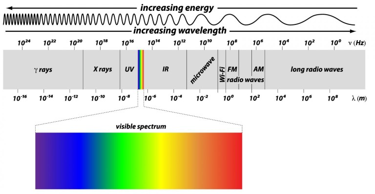
EUV stands for "Extreme Ultraviolet". It refers to the wavelength of light. The wavelengths of deep ultraviolet (DUV) light used in chip production are 248 and 193 nm, while the wavelength of light used in EUV lithography is 13.5 nm.
- EUV Lithography Systems
EUV (Extreme Ultraviolet) lithography uses an EUV light of the extremely short wavelength of 13.5 nm. It allows exposure of fine circuit patterns with a half-pitch below 20 nm that cannot be exposed by the conventional optical lithography using an ArF excimer laser.) Putting it into practical use requires a variety of element technologies, including the light source, optics, masks, photoresist, and lithography tools.
Among these element technologies, the biggest challenge is the technology that generates a powerful EUV beam of the extremely short wavelength of 13.5 nm. This EUV beam can be taken out from high-temperature and high-density plasma.
Two methods are used for producing plasma: the Laser-Produced Plasma (LPP) method that produces plasma by condensing a strong laser beam onto a certain material, and the Discharge-Produced Plasma (DPP) method that produces plasma by a pulsed high-current discharge between electrodes in an atmosphere of certain materials.
The EUV beam exiting from the plasma is collected by the condensing mirror, passes through a point called the intermediate focus (IF), and illuminates a reflection-type mask after it has been reshaped by the illumination optics. The EUV beam reflected by the mask is exposed by the projection optics to form a pattern on photoresist that is coated on a wafer surface.


